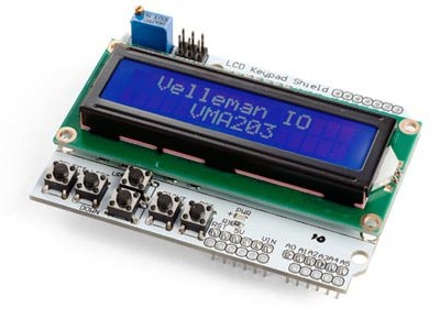
LCD and KeyPad Module
(Fully Assembled PCB)
Product Use
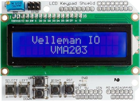
This 5 VDC LCD and KeyPad Module is especially developed for Hobby use, allowing microcontroller to be commanded by use of any of the five KeyPad switches.
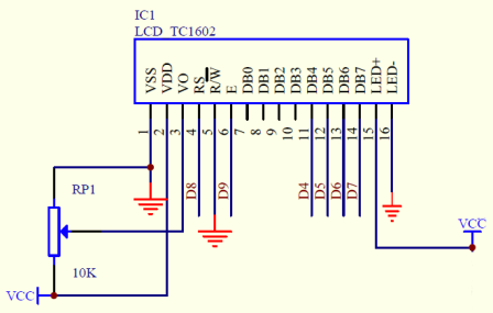
The 16 character 2 row LDC display has LED backlight and also has manually adjustable contrast via on Module multi-turn trim potentiometer.
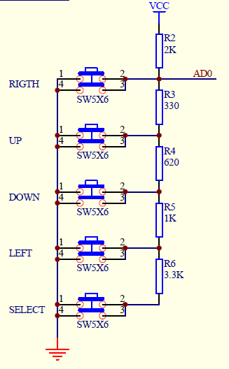
Command Signal from the 5 KeyPad switches is sent via single Analog Data Line D0 to Analog to Digital Converter (ADC) and the generated Voltage Level is then interpreted by the microcontroller.
The Module only requires about 30mA at 5VDC.
The Red LED located on the PCB is ON when the Vcc Power Input Pin is connected to +5VDC.
The LCD Control Inputs can be connected directly to any output pin of PARALLAX PROPELLER microcontroller without need for any resistors or Voltage translators.
The 5 VDC LCD and KeyPad Module is also Arduino Compatible.
Features
- Control LCD Module with a six high/low Command signals
- Power ON Monitoring Red LED
- Nominal Voltage 5V
- Screen Contrast Adjustment
- Blue background / White LED backlight
- 5 KeyPad buttons
- Up, Down, Left, Right and Select buttons use only one analogue output A0
Connections
INPUT
- Vcc +5 VDC
- GND (Common System Ground)
- RS=D8 RECEIVE INSTRUCTION OR DATA
- E=D9 Data ENABLE
- D4-D7 DATA BUS LINES
- D10 Back Light DISABLE (Optional)
OUTPUT
- KeyPad = A0
- GND (Common System Ground)
Product Specifications
| Power source voltage (min/max) | VCC | 4.5 / 5.5 | V |
| Command Signal Voltage (min/max) | VS | 3 / 5 | V DC |
| Power Consumption (LED and LCD) | Pon | 145 to 160 | mW |
| Operating Temperature | Ton | 20 to 140 -6 to 60 |
°F °C |
| Dimensions | 80 x 58 x 20 | mm |
Module Circuit Diagram
KeyPad
LCD
Connectors
TOP Connectors:
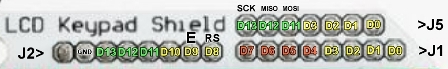
NOTE: Pins on TOP Connectors numbered from Left (1) to Right (n)
| Pin Function | Connector-Pin | TC1602 |
|---|---|---|
| DB7 - DATA BUS LINE 7 (MSB) | J1-1 | D7 |
| DB6 - DATA BUS LINE 6 | J1-2 | D6 |
| DB5 - DATA BUS LINE 5 | J1-3 | D5 |
| DB4 - DATA BUS LINE 4 | J1-4 | D4 |
| DB3 - DATA BUS LINE 3 | J1-5; J5-4 | D3 |
| DB2 - DATA BUS LINE 2 | J1-6; J5-5 | D2 |
| DB1 - DATA BUS LINE 1 | J1-7; J5-6 | D1 |
| DB0 - DATA BUS LINE 0 | J1-8; J5-7 | D0 |
| Not Connected Not Used | J2-1 | |
| Vss - POWER SUPPLY (GND) | J2-2 | Vss |
| - BACKLIGHT DISABLE (if Grounded) 5mA | J2-6 | D10 |
| E - ENABLE SIGNAL | J2-7 | D9 |
| R/S - FLAG TO RECEIVE INSTRUCTION OR DATA
0 - INSTRUCTION 1 - DATA |
J2-8 | D8 |
BOTTOM Connectors:
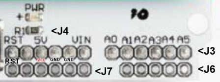
NOTE: Pins on BOTTOM Connectors numbered from Right (1) to Left (n)
| Pin Function | Connector-Pin | TC1602 |
|---|---|---|
| AO - Buttons Analog Output | J3-6 | |
| Vss - POWER SUPPLY (GND) | J4-2/3; J7-2/3 | Vss |
| Vcc - POWER SUPPLY (+5V) | J4-4; J7-4 | Vdd |
Pricing
US $10.00 each